
LKC FES student won BESA 2020


Tain (left) and Ts Dr Wong (right)
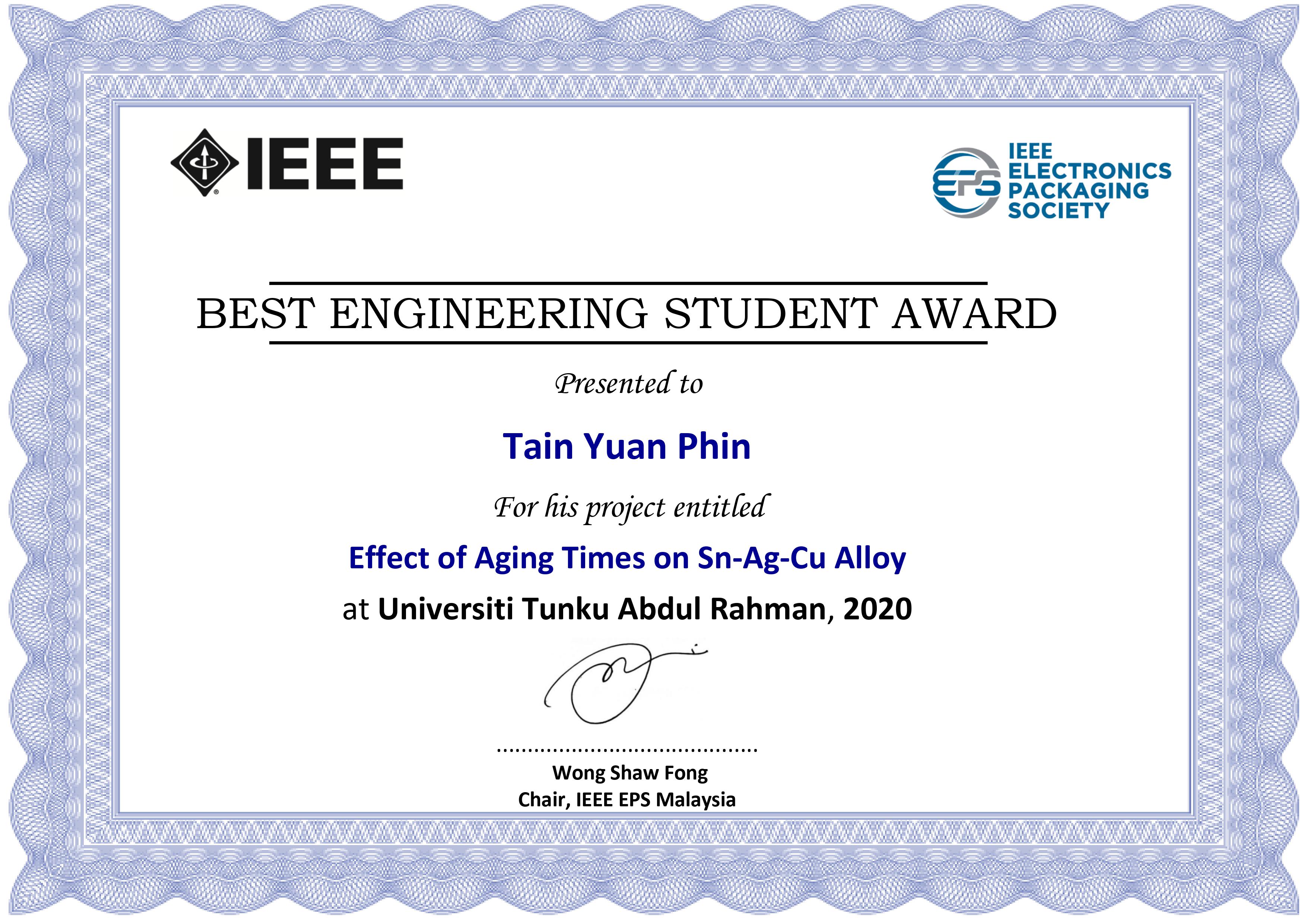
Lee Kong Chian Faculty of Engineering and Science (LKC FES) student Tain Yuan Phin won the “Best Engineering Student Awards (BESA) 2020” organized by IEEE-EPS Malaysia. In his final year project titled, “Effect of aging times on Sn-Ag-Cu alloy”, a patented (Malaysia & International patents) SAC-Pt alloy was used to compare against the commercial SAC solder to study the microstructural evolution after different reflow times as well as during isothermal aging. Tain was supervised by LKC FES Department of Mechanical and Material Engineering Ts Dr Wong Mee Chu.
Tain, who studied Bachelor Of Engineering (Honours) Materials And Manufacturing Engineering said, “It is indeed a great honour and privilege for me to receive the BESA award from IEEE-EPS and it certainly helped in improving my self-confidence. I want to express my gratitude towards the organiser and UTAR for giving me the opportunity to take place in the competition. I would also like to thank my supervisor, Ts Dr Wong Mee Chu for her great support by providing proper guidance and emotional support along the way. I am grateful to my parents and my friends that helped me in one way or another along the journey.”
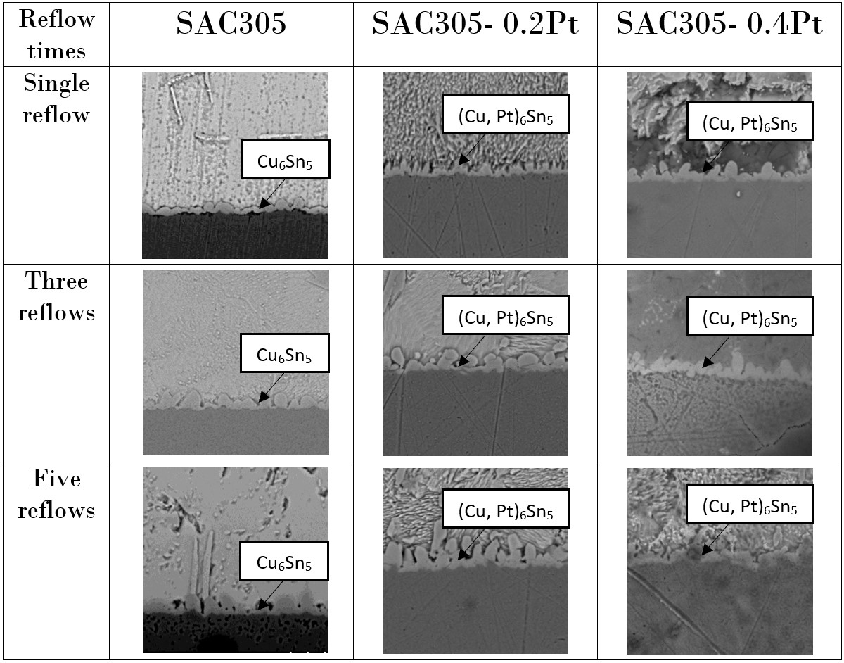
The table shows the micrographs under the Scanning Electron Microscope of IMCs without heat-aging. The IMC layer at the SAC305-Cu interface is identified as Cu6Sn5 while for SAC305-Pt joints, the IMC layers are composed of (Cu, Pt)6Sn5. For single reflow, the IMC layers are scallop-shapes which coarsened after multiple reflows due to Ostwald ripening
The thick intermetallic compound (IMC) forming at the SAC solder/substrate interface is inherently brittle, compromising structural and electrical integrity. Pt particles were mechanically mixed into a commercial SAC solder paste before stencilling on a Cu substrate. The substrate was ultrasonically cleaned and pre-coated with RMA flux before the reflow soldering process. Isothermal aging was carried out at 150°C. The samples were subjected to standard metallographic preparation before imaging and analysis using the scanning electron microscope with EDX.
In the study, it was found that multiple reflows led to thicker and coarser scallop-shaped IMC layers in the commercial SAC solder joint. When Pt reinforcement between 0.20-0.40 wt.% was added, the IMC layer was suppressed. Kirkendall voids were present in SAC samples with increasing reflow times as well as after isothermal aging. These voids were noticeably reduced in Pt-containing joints. This is attributed to the formation of the (Cu,Pt)6Sn5 compound on the IMC layer, which slowed down the interfacial diffusion process and thus controls the excessive growth rate.
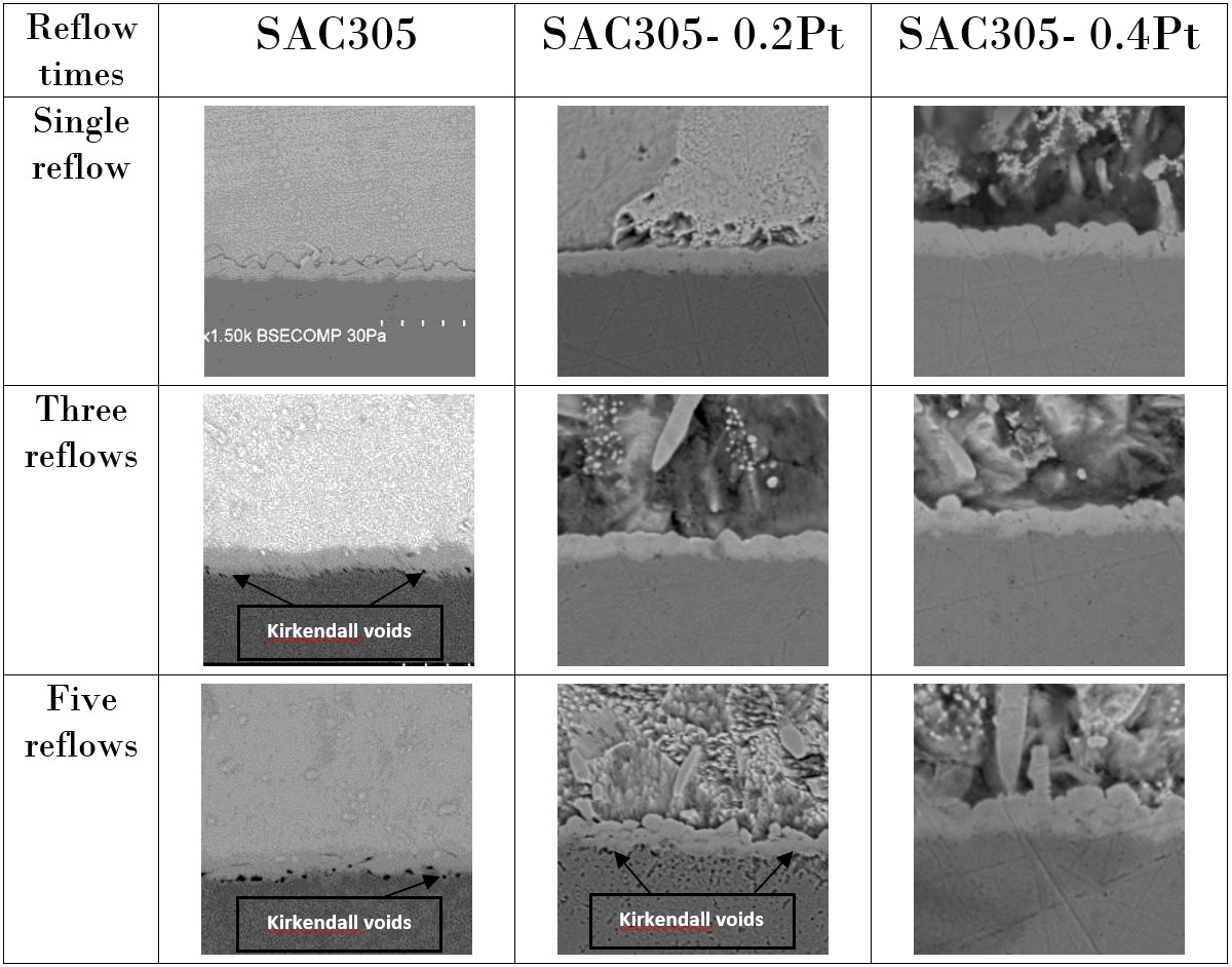
Microstructure of IMCs under SEM after 72hrs isothermal aging
“Soldering is an essential process to connect electrical components and conventionally used solders contained Lead that is harmful to the environment and human health. Therefore, the Lead-free Sn-Ag-Cu (Tin-Silver-Copper) solders served as an alternative solder alloy system. However, the prevalent issues hampering the successful application of the Sn-Ag-Cu solders in electronic packaging are largely attributed to the excessive intermetallic compound (IMC) layer growth and the presence of Kirkendall voids which both will lead to electrical and mechanical failure. These situations are further aggravated due to the miniaturization of the electronic package. Pt (Platinum) has a large atomic size and is an excellent electrical conductor and has been conventionally used as diffusion barrier in the metallization layer of the electronic package. In this study, Sn-3.0Ag-0.5Cu solder alloys reinforced by 0.20 wt.% (weight percentage) and 0.40 wt.% Pt were reflowed onto empty printed circuit boards (PCB) between one to five times, followed by accelerated heat-aging for up to 168 hours. Multiple reflows stimulate the stacking of chips during electronic packaging and accelerated heat-aging stimulates heat in the electronic devices during the in-service lifespan. It was found that multiple reflows and heat-aging lead to the thickening of IMC layer and the formation of Kirkendall voids. Besides,0.20wt.% Pt suppressed the thickness of the IMC layer while the presence of Kirkendall voids were significantly reduced when 0.40wt.% Pt was added. The (Cu,Pt)6Sn5 IMCs formed when Pt was added to Sn-3.0Ag-0.5Cu solder is believed to control the excessive IMC layer,” explained Tain on his project.
Tain enthused, “Begin, even if you have no idea if it will work.” “The final year project is the last step before graduation. It's a great opportunity for students to apply what they learned throughout the tertiary studies. The skills learned while completing your project will certainly help you in the near future if you were to enrol in the field related to your course. Do not be afraid to approach your supervisor for consultation when facing obstacles or challenges. Try to voice out how you can improve your final year project title and the Design of Experiments. Your supervisor is professional and is always there to back you up. Please do enjoy your time doing your final year project, do not be too stress and always try your best,” added Tain.
Tain and Ts Dr Wong expressed their appreciation to the Ministry of Science, Technology and Innovation of Malaysia for the funding of the project under the eSciencefund.
Tain received RM 3,000, which part of it will be used to sign up IEEE and IEEE EPS membership, and purchase a book by IEEE EPS Malaysia Chapter. The book will be donated to the UTAR’s library under Tain’s and IEEE EPS Malaysia Chapter.
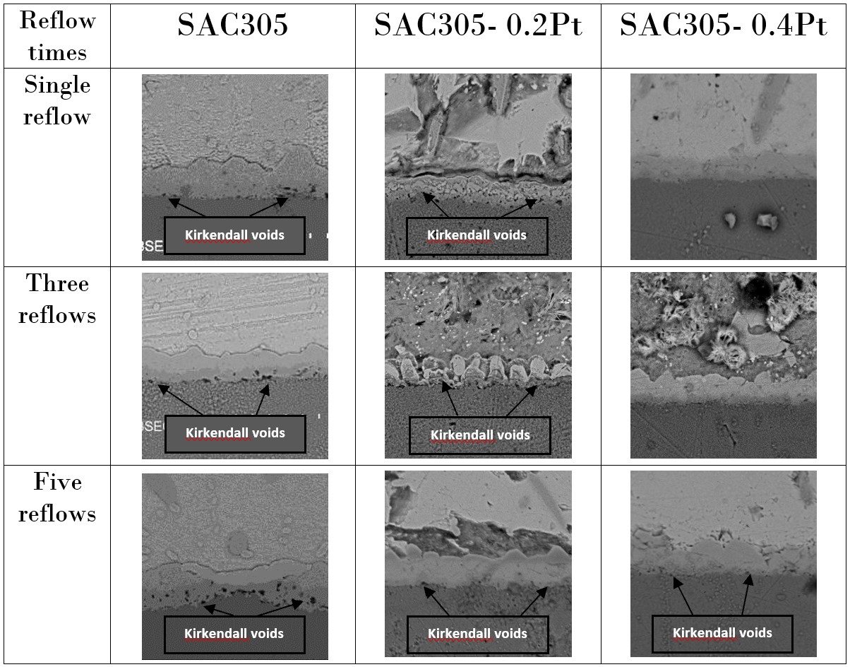
Microstructure of IMCs under SEM after 168hrs isothermal aging
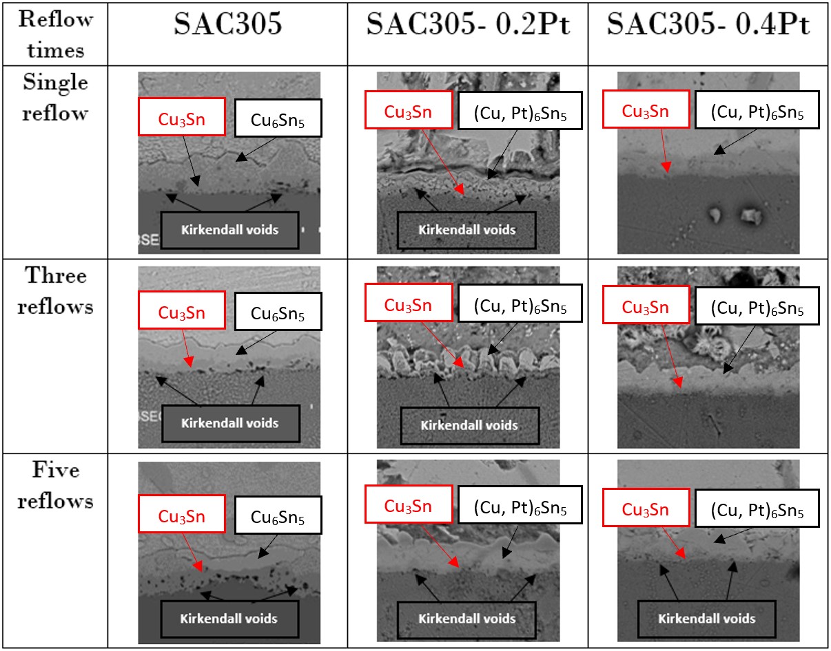
Microstructure of IMCs under SEM after 168hrs isothermal aging (layer labelled)
Tain's BESA 2020 certificate
© 2020 UNIVERSITI TUNKU ABDUL RAHMAN DU012(A).
Wholly owned by UTAR Education Foundation Co. No. 578227-M LEGAL STATEMENT TERM OF USAGE PRIVACY NOTICE